Creating round (arc) copper planes [SOLVED]

I used that just as a ‘quick hack’ and had to modify the code all the time to get the output I wanted/needed, so it appeared in the python console in my WingIDE and from there it was just copy&paste into the kicad_pcb.

If I run it in command line in windows the following way:

E:\Data_Code\Python\KiCAD_CopperArc>KiCAD_CopperArc.py > CopperArc.txt

the result will be in CopperArc.txt and you can copy&paste from there?

hi,
finally got it up and running :slight_smile: the result looks like this:


but how do I get from there to a pad that looks like this:

even drawing two arcs and connect them with two straight lines will not give me a solid copper plane. Do you think the script can be modified to fit the xy format of a polygon?

(pts
(xy 167.64 90.17) (xy 172.72 90.17) (xy 172.72 93.98) (xy 167.64 93.98)
)

because then I would have a solid plane that can be assigned to a net I want.

thanks for your effort!

Try this one…
KiCAD_CopperFillPoly.py on Github Gist

It needs a premade polygon/fill area where you replace the polygon and filled_polygon parts. My KiCAD didn’t want to fill the area unless I had the net really connected to it with a pad or some wire, thus I also let it output the filled_polygon part so you don’t panic - but this doesn’t survive a ‘Fill or Refill All Zones’ command…
You need to figure out how to get the refill to work though, as for those holes you either have to program them into the output (I won’t be doing that, sorry) or you have to let KiCAD do the work, but for that it needs some net connected to the filling area via pad or wire of the same net being in the to-be-filled-area.
But it’s not that hard anyway, a simple DIY SMD pad with just 1 pin and that being on the GND net will be the easiest (start in eeschema for that one to get the netlist right).

Almost there :smile:
I tried the script and it just needs some minor modifications to fit my needs. Currently the script is just drawing one arc:


but I would need to have the option to define a innerRadius and a outerRadius to get the pad shape. The calculation will stays the same but the for loop that calculates the coordinates must run a second time with the other radius value.
I did this manually and it turned out like this:

there is just one thing you need to consider, the coordinates of the second arc needs to be in reverse order to get the shape right. Otherwise it will turn out like this:

I guess this modification can be done very quickly, but if you don’t want to spend time on this I will try it by my own.

Anyway thank you for your effort, you already helped me a lot.

cheers!

To go the other way round you probably need to add a minus in front of the i and you would need to adjust the startangle value with the angle value :

    pointX = baseX + radius * math.sin(math.radians(sideangle*(-i+0.5) + (startangle - angle))
    pointY = baseY + radius * math.cos(math.radians(sideangle*(-i+0.5) + (startangle - angle))

Yeah, will get you there, didn’t test it, don’t intend to, good luck :slight_smile:

Hey Joan,
I finally was able to made the necessary changes :smile: and it works like a charm
KiCAD_CopperFillPoly.py (1.6 KB)

import sys, os
import shutil
import math

LIST_pts = [" (polygon\n (pts\n (xy “,” (filled_polygon\n (pts\n (xy “,”) (xy “,”)\n )\n )"]

def FNC_poly (cntr, # (x,y)
innerRadius,
outerRadius,
sides,
startangle,
angle,
):

STR_data = ""
baseX = cntr[0]
baseY = cntr[1]
sideangle = angle / sides
for i in range(sides):
    pointX = baseX + innerRadius * math.sin(math.radians(sideangle*(i+0.5) + startangle))
    pointY = baseY + innerRadius * math.cos(math.radians(sideangle*(i+0.5) + startangle))
    STR_data += "{:.4f}".format(pointX) + " " + "{:.4f}".format(pointY) + LIST_pts[2]
for i in range(sides):
    pointX = baseX + outerRadius * math.sin(math.radians(sideangle*((sides-i-1)+0.5) + startangle))
    pointY = baseY + outerRadius * math.cos(math.radians(sideangle*((sides-i-1)+0.5) + startangle))
    STR_data += "{:.4f}".format(pointX) + " " + "{:.4f}".format(pointY) + LIST_pts[2]
STR_data = STR_data[:-6] + LIST_pts[3]
return LIST_pts[0] + STR_data + "\n" + LIST_pts[1] + STR_data

if name == ‘main’:

Center = [100.0,100.0] # x/y coordinates of the centre of the pcb sheet
innerRadius = 6 # mm
outerRadius = 7.5 # mm
Sides = 20
StartAngle = 75.0 # degrees
Angle = 30.0 # degrees
print FNC_poly (Center,
                innerRadius,
        outerRadius,
                Sides,
                StartAngle,
                Angle,
                )

thank your for your help!
I also want to provide a short how to for other people using this script.
1. open the script with the editor of your choice and change the parameters innerRadius, outerRadius, Sides, StartAngle and Angle to your needs. Save it!
2. under windows, navigate to the folder where the python script is stored and use the command: yourPythonScriptName.py > yourDesiredOutputFile.txt
to get the output data stored in a text file
3. open your PCB file and draw a simple polygon (shape doesn’t matter here) save it and close it
4. open your .kicad_pcb file with an editor and detect the polygon you’ve drawn earlier, this looks something like this:

(zone (net 1) (net_name +3V3) (layer F.Cu) (tstamp 0) (hatch edge 0.508)
    (connect_pads (clearance 0.2))
    (min_thickness 0.254)
    (fill yes (arc_segments 32) (thermal_gap 0.508) (thermal_bridge_width 0.508))
    (polygon
      (pts
        (xy 105.8154 101.4769) (xy 105.8521 101.3242) (xy 105.8847 101.1705) (xy 105.9133 101.0161) (xy 105.9379 100.8610) (xy 105.9584 100.7052) (xy 105.9748 100.5490) (xy 105.9872 100.3924) (xy 105.9954 100.2356) (xy 105.9995 100.0785) (xy 105.9995 99.9215) (xy 105.9954 99.7644) (xy 105.9872 99.6076) (xy 105.9748 99.4510) (xy 105.9584 99.2948) (xy 105.9379 99.1390) (xy 105.9133 98.9839) (xy 105.8847 98.8295) (xy 105.8521 98.6758) (xy 105.8154 98.5231) (xy 107.2692 98.1539) (xy 107.3151 98.3448) (xy 107.3559 98.5368) (xy 107.3917 98.7299) (xy 107.4224 98.9238) (xy 107.4480 99.1185) (xy 107.4685 99.3137) (xy 107.4839 99.5095) (xy 107.4942 99.7056) (xy 107.4994 99.9018) (xy 107.4994 100.0982) (xy 107.4942 100.2944) (xy 107.4839 100.4905) (xy 107.4685 100.6863) (xy 107.4480 100.8815) (xy 107.4224 101.0762) (xy 107.3917 101.2701) (xy 107.3559 101.4632) (xy 107.3151 101.6552) (xy 107.2692 101.8461)
      )
    )
  )

5. open the output text file of the script and copy the section (pts…) looks something like this:

(pts
        (xy 105.8154 101.4769) (xy 105.8521 101.3242) (xy 105.8847 101.1705) (xy 105.9133 101.0161) (xy 105.9379 100.8610) (xy 105.9584 100.7052) (xy 105.9748 100.5490) (xy 105.9872 100.3924) (xy 105.9954 100.2356) (xy 105.9995 100.0785) (xy 105.9995 99.9215) (xy 105.9954 99.7644) (xy 105.9872 99.6076) (xy 105.9748 99.4510) (xy 105.9584 99.2948) (xy 105.9379 99.1390) (xy 105.9133 98.9839) (xy 105.8847 98.8295) (xy 105.8521 98.6758) (xy 105.8154 98.5231) (xy 107.2692 98.1539) (xy 107.3151 98.3448) (xy 107.3559 98.5368) (xy 107.3917 98.7299) (xy 107.4224 98.9238) (xy 107.4480 99.1185) (xy 107.4685 99.3137) (xy 107.4839 99.5095) (xy 107.4942 99.7056) (xy 107.4994 99.9018) (xy 107.4994 100.0982) (xy 107.4942 100.2944) (xy 107.4839 100.4905) (xy 107.4685 100.6863) (xy 107.4480 100.8815) (xy 107.4224 101.0762) (xy 107.3917 101.2701) (xy 107.3559 101.4632) (xy 107.3151 101.6552) (xy 107.2692 101.8461)
      )

6. go to your kicad_pcb file and replace the coordinates. save it.
7. done! if you open kicad again your polygon should look similar to this:
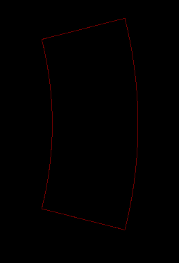
as mentioned earlier in this thread you need to connect or place a component inside the polygon to be able to fill it.

All credits here goes to @Joan_Sparky for making this cool script.

1 Like

My situation was not similar to yours, but since I came here googling arced/curved ground planes I just want to show what the solution was for me, so no one in my situation thinks he needs scripting to solve it.

I basically had a square outline with curved notches, and was looking for a way to trace the outline curve with ground plane. Turns out I got away with just drawing the outline on the absolute outline border and the ground plane was restricted to my board outline and therefore curved itself.

1 Like

That is normal behavior… you can even do this (without the help of the edge.cuts layer):

But it will be pretty tiresome to draw something like the OP needed with different edge radii and other shapes…

Hi,
I’ve been using the python script KiCAD_CopperArc.py to create some round tracks. I’m using python 2.7.14 and kicad 4.0.6. The problem is that the tracks I generate are shown by pcbnew but don’t belong to the net I am assigning them, they are all inserted to the “net [] (0)”, even if in the .kicad_pcb file the net is (net 1).

I tried to change the position of the added tracks inside the .kicad_pcb file from the end of the file to the “segment” section (it seems that the tracks generated by kicad are ordered according to the number of their associated net) but the problem is not solved.

Maybe I’m not using enough fiddling and determination but I really don’t know what else can be done apart from changing the position of the inserted tracks. Do you have any ideas?
Thank you

Does your kicad_pcb file have a netlist assigned to it, or is it a blank/new one?
You need something like this to appear in that file, then the net assignment should stick:

      ....
      (subtractmaskfromsilk false)
      (outputformat 1)
      (mirror false)
      (drillshape 0)
      (scaleselection 1)
      (outputdirectory gerber/))
  )

  (net 0 "")
  (net 1 GRD)
  (net 2 SNS)
  (net 3 HV)
  (net 4 0V)
  (net 5 +UB)
  (net 6 "Net-(D8-Pad2)")
  ...

Thinking about it some more, it would help to have a copper track going to a pad with the same net that you assigned.
So the track isn’t considered loose and it’s netclass reduced to zero.

If you start PCBnew, a way to get around this is to disable DRC… then create that connecting track… then save the whole thing… and then activate DRC again.

Soemthing along those lines equals fiddeling + determination.

1 Like

The .kicad_pcb file had a netlist assigned. I solved the problem disabling the DRC and drawing a copper track ending exactly at the beginning of the curved tracks, before the adding of the curved tracks themselves.
Thank you very much for the fast and useful answer!

1 Like

Another solution is to run KiCommand, but it requires the nightly version at this point.

Works with nightly

WARNING: The nightly version is not guaranteed to produce files that can be opened in the stable version. There is not even a guarantee that one nightly build can open the files produced by another nightly build. (In most cases there is no problem but you might encounter one. Just know the dangers that come with using a development build.)

It can create regular polygons with as many edges as you want to draw. Then you can use the ‘regular’ command to make it a regular polygon (equal edges, equal angles). At this point, it’s only on drawable layers, not copper, yet. But you can get the points you need from the file after saving. Then maybe change it to a copper track afterwards.

Use ‘regular’ then delete the segments you don’t want. I find 32-64 segments is close to a circle.

Future commands will make creating copper nets possible directly.

I am laying out a circular PCB with a series of twelve pie-shaped wedges, every 30 degrees, for an electrostatic sensor. At first I used Inkscape and svg2mod to create the whole thing as a custom footprint. This used the “fp_poly” command in the footprint, and I added a small square pad inside each wedge so there would be something to connect to.

This worked great, except that I have parts mounted on the other side of the PCB, and I need to use a few vias to connect to inner layers (this is a four-layer board). Because the footprint “zones” are not real kicad filled zones, kicad won’t clear a ring around my vias where they protrude into my sensor footprint, and they will short out. Bummer.

So I found this thread and decided I would be just as well off (maybe better) using proper “filled zones” generated with the poly version of the python script developed above (thanks!). There are just two problems:

  1. My board is 10 cm in diameter, so the 32-segments-per-360-degrees limitation is a real problem. The python script makes a really nice pie-wedge-shaped zone, but as soon as kicad refills it for any reason, the nice curved edge goes away and is replaced with a very jagged edge.

  2. I want to push the copper as close as I can to the edge of the board. AFAICT the only way to accomplish this is to change the global “clearance” parameter for the zone, but this also affects the clearance to tracks and vias, which, unlike the board outline, I do need to be careful of.

Issue #1 is exacerbating issue #2, because the clearance to Edge.Cuts is determined by the joints in the line-segment approximation to the curve. Because that is such a crude approximation on a 10-cm circle, the actual clearance from most of the copper to the board edge ends up being considerably more than the nominal clearance.

I would create a circular ring to fill to the board edge, and use regular zone to fill in the rest. Unfortunately you can’t draw directly onto copper layer, so you would have to create a footprint. It’s a bit of hack, but can’t think of a better way.

I guess if you are editing the kicad_pcb file directly, you can also draw on some other layer then edit the layer.

That doesn’t really work :frowning:

Perhaps create a circular ring of pads in a footprint, not sure that would work either. How much do you need it?

I did a quick test and it appears to work

I would use a script to create a complete ring.

BTW, it would be better to start a new thread and reference other related ones, rather than tag on to old threads especially when they are marked “solved”.

Thanks bobc. I’m new and didn’t realize there was a solved/unsolved system. I’ll start a new thread if I need more help.

The circular ring of pads is a clever idea. An ugly hack, but, pretty much all of the solutions I’ve come up with fall into that category. What I’ve learned is that kicad does not always take my round edge (from the script-generated filled_polygon points) and turn it into a jagged one. It only does so when the jagged edge would violate the clearance at Edge.Cuts. This leads to some very strange looking effects where, as you change the zone clearance value, parts of the curve stay nice and round while other parts get ruined by the “rule of 32”. But it also opens up a workaround (I think):

If I temporarily move my circular board outline out by a millimeter, and generate the zones using the python script to the true outer edge, they won’t be clipped; they stay round. I’ve tried adding vias, traces, etc. and it seems that the redraws/refills of the zone don’t destroy this, since the zone is no longer clipped at the edge. My plan is to finish the board, remembering to keep > 1 mm back from the “fake edge”, then generate gerbers, then move the board edge back to the correct position, generate just the Edge.Cuts gerber, and swap that out.

Presumably, it’s a big hassle to extend the code to support > 32 segments, or it would have happened already. But with fast CPUs and lots of memory commonplace nowadays, I wonder if the 16/32 choice could be changed to something else, like 32/128 or 64/256? That would be a reasonable stopgap until a better solution is implemented.

This was exactly what I needed- I didn’t know it would do this. Thanks!! :grinning:

Hey, iam at this Point, but i don´t know what i have to do next……

thanks in Advance for help

Please start a new thread and describe your situation. I’m not going to read through a 5 year old long thread to find out what it’s about. (KiCad changes rapidly, UI is different, functionality may be different… and the thread has probably evolved over time.)

I solved it thank you…^^ I had to run the Code in CMD Window copy the .txt file and paste in to den txt file of the pcb file.