Create Copper Zone from Outline

Hello guys,
at the moment i am trying to import the Edge.Cut Layer / board outline of a pcb from a .dxf file, which works fine so far.
But i am struggling with the next step, the conversion of the outline to a copper zone, e.g. for a ground layer.
I cant find a way in KiCad to change a Edge.Cut layer into a copper zone.
You can change the Edge.Cut layer into a polygon, but only into a non copper polygon.

I found a workaround to modify the .kicad_pcb file and change the layer manually to a copper layer,
but i am wondering if there is no solution for this in the PCB Editor.

The KiCad Version is 6.0.9

Thank you
Dennis

Draw a ground plane around the edges of Edge.Cuts. KiCad ist smart enough to only fill the PCB as defined by the Edge.Cuts layer.

I usually draw some kind of pentagon or paralellogram around the PCB, and then let the PCB editor clip the copper zones by the Edge.Cuts lines.

The reason it’s just some weird shape has a few reasons:

  1. It’s the quickest way to draw it. no need for messing with precise coordinates.
  2. Zone boundaries do not overlap, so a zone edge is very easy to select with the mouse.
  3. If you see the weird shape turn up in a Gerber file, you immediately know there is something wrong with the Edge.Cuts layer which needs attention.

+1 for the “draw gnd-zone bigger than board-outline” (it’s the fastest/easiest way).

Nevertheless, if you still want the gnd-zone to exactly match the board-outline:

  1. requirement: assuming the board-outline is a closed polygon on edge.cuts
  2. select polygon
  3. select F.Cu-layer on right appearance panel
  4. RMB-click → context-menu → Create from selection → create zone from selection
  5. you now get the standard zone-creation-dialog. Be sure to set at least a correct zone-priority, all desired copper-layers (top/bottom/inner layers - as you wish) and the zone-net.
  6. OK to close zone-creation-dialog and look → a new zone has turned up
1 Like

Additional, this does indeed not work:

You can create a zone from an imported dxf, but it has to be on a copper layer.

In addition to what others have said, a ground plane or other copper area must not reach the board edge. It needs clearance. So, you can’t just copy the board outline.

Why shouldnt I set the copper outline and the board outline on the same outline in KiCad?
You can set the “Copper to hole clerance” and “Copper to edge clearance” of your manufacturer in your Borad Setup.

This is the problem. You cant select a copper zone in the dialog, only “Non Copper Zones”.

grafik

have you followed the description exactly? step 3 (select F.Cu as active on appearance panel) is very very important! (I had extra tested my suggestion yesterday - and it worked on my computer. Kicad v6.0.9 on win10).

If it still doesn’t works I would be interested in your dxf-file and/or the archived kicad-project - so I could try if some other settings are influencing the conversion-tool.

1 Like

That is because copper zones can only exist on copper layers.
You have to move your graphics to a copper layer first.

I am experimenting a bit with this on KiCad V6.0.9 myself right now, and there seem to be some interference between a dxf imported as a block (which is default) and creating a copper zone from it, but as you can see in the screenshot, it works at least partially.

Also note that the zone has to reach a pad for it to fill at all. (with the B shortcut key).

Oh, I’m sorry. If it’s a zone it obeys the clearance. But as others have said, there’s no need to follow the outline exactly because it’s easier to just draw a larger polygon.

In general, I dislike putting lines (or any other items) on top of each other. It makes it more difficult to select them, and it creates room for confusion.

I’ve made a little test project because I appear to bump into some strange or buggy behavior I do not understand.

First, the schematic, nothing special, just something to make KiCad happy:

Then the PCB.
It has two copper zones. The blue one on the back is clipped by Edge.Cuts, and as you can see, it keeps a clearance from the edge. This is quite important, as a copper zone that goes to the edge can create shorts, either by “smearing” of the copper to other layers, or when the PCB is in touch with some metal enclosure. Same for mounting holes and metal screws etc.

For the other zone:
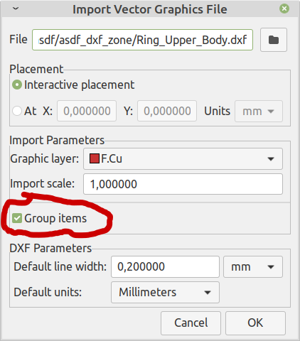
First import it: PCB Editor / File / Import / Graphics / Ring_Upper_Body.dxf and make sure to put it on a copper layer (In this case F.CU).

Bug 1: Right after that I find the fist bug or missed feature.
I have imported the graphics as a group:
image

But the “Create from Selection” entry is missing from the popup menu. To be able to make the screenshot below, I first had to “enter” the group, which also selects the items in the group.

When I’ve entered the group, I can create a zone from the items in the group. Here added the newly created zone to the “GND” net, and placed it over the corresponding connector pins.

Bug 2: I’ve created a zone from the imported DXF, but it keeps a clearance from the edge of the DXF. Is this a bug or a feature?

Bug 3: I can not draw a copper track from the GND pin of J2 to J1 because KiCad does not let me cross the boundary of the DXF.

Bug 4: It’s quite difficult to see whether you’re in “group editing mode”, I guess that especially when there are nested groups it’s confusing on which level you are.

Note that I’m not very familiar with DXF import in KiCad, and creating zones from imported graphics is also a relatively new feature. So it could be either misunderstandings, or bugs. I’ve also not looked on gitlab (yet) for existing bug reports concerning these issues.

To reduce the amount of time needed for others to have a look at this, I’ve attached the project, including the original DXF file.

2022-11-16_asdf_dxf_zone.zip (25.8 KB)

The DXF was created by FreeCAD.

bug1: create zone from group - this is currently just not supported. As a group can contain many different items (also items of different types) I find this restriction resonable.
bug2+3: the original imported graphics are on F.copper. Every track/zone-fill has to respect the copper-copper-clearance. So no bug.
bug4: understandable.

Ah, indeed.
I forgot that “Create Zone from Selection” just creates a new zone, and preserves the original graphics. So both Bug 2 and Bug 3 are a result of this. If I move one the arc of the graphics then the zone both refills to it’s edge, and I can enter the zone with a track:

Just to add, because this is a handy but non-obvious feature, when you use “Create X from selection” the original item is preserved and remains selected. So if you want to delete the original item after creating a new item, you can just hit delete immediately after creating the new item.

2 Likes

This topic was automatically closed 90 days after the last reply. New replies are no longer allowed.