I am trying to pickup some kicad experience. have been working with other programs, latest AutoraxDEX, while waiting for KiCad to pickup abilities.
A random experiment with the Footprint Editor have landed me in trouble making a new FP using the Wizard.
I have done limited searching on Forum [not really familiar with the environment here yet] but not yet found a solution.
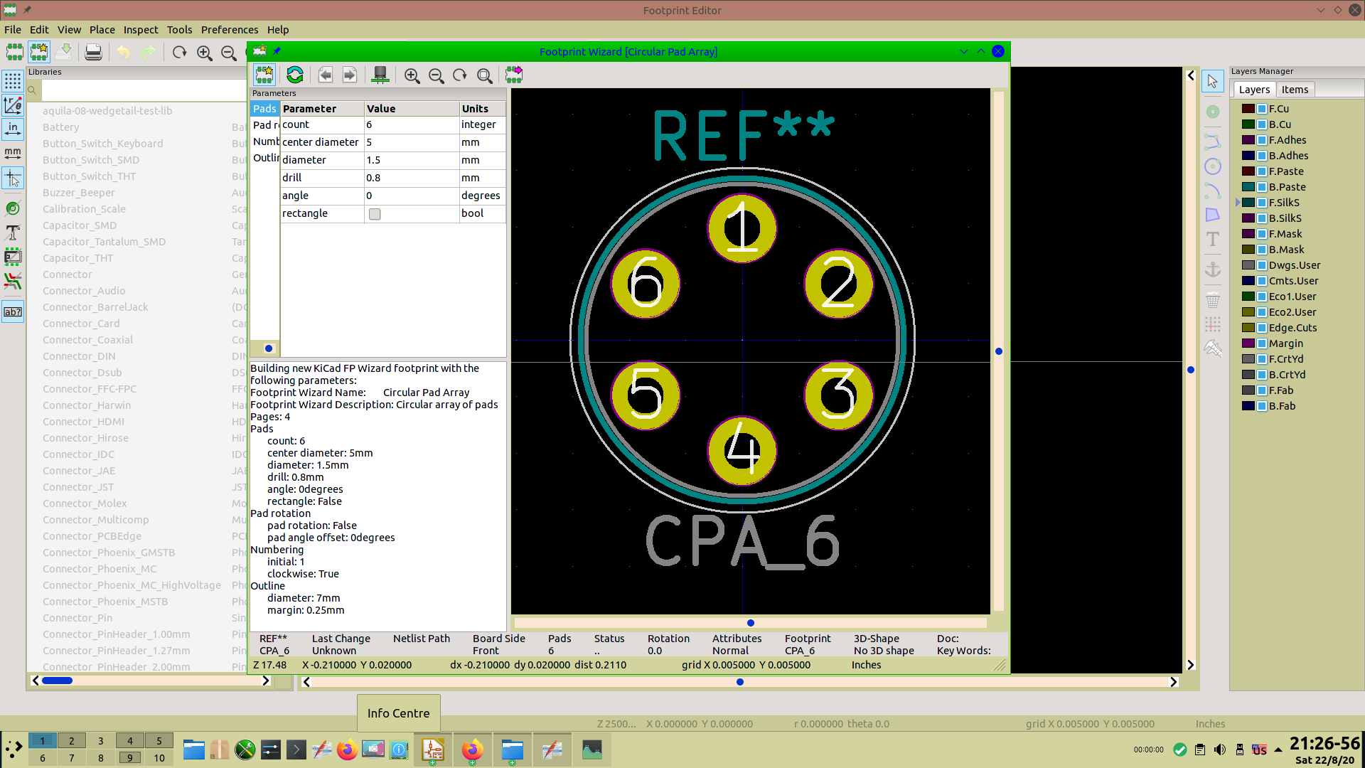
Trying to use the parametic design of a circular array of 36 pads. In the example I am attaching if I can the array has 10 pads. The problem arises when setting to array radius to more than 5 mm the pads seem to evaporate. The 3D viewer just shows a piece of pcb.
Then I kept the radius at 5mm and exported the FP to the Editor and can then Edit normally I it seems.
However I wanted have 36 pads on much bigger radius so it would be nice if the parametrics can handle this.
If you use wizard 1 “Circular Pad Array” and use parameters that the wizard thinks does not make sense, it spits out an error message and refuses to draw the footprint.
If you set the radius of the pads too big then it says:
So if you then go to the “outline tab”, and increase the diameter of the outline:
Also:
The way the parameters are presented may seem a bit clunky, but it’s because the footprint wizard scripts are also relatively simple python scripts.
If you intend to use these often, and/or need some functionality that is missing it should be fairly easy to copy such a script and use it as an example to modify it into your own.
On my Linux box the scripts are in:
/usr/share/kicad/scripting/plugins/
Do note though that this location is not normally writable by users, and if you add scripts there they will get overwritten or removed with KiCad updates.
The KiCad manual is very short on the wizard scripts, but does suggest that you can also put them in other locations (I have not tried this)
All of KiCad’s file formats are simple readable ascii.
A few years ago I was experimenting with Python, and combined with the description of file formats, I wrote a script that generated a library with some 40+ connectors, with different amount of pin numbers.
More about KiCad’s file format’s on: https://kicad.org/help/legacy_file_format_documentation.pdf
paulvdh
Thank you for replying. I now understand what happened. I was a bit rattled because I did not understand why I had missed the little panel where you show the ‘outline’ . Sounds silly that was what I was looking for.
Then I discovered I have an odd behaviour dpending on the window size. As shown in the attachement.
Yes you could say it is a bit clunky but since it is work in progress I have no problem with putting up with having to use it.
At the moment python is not for me but the having files in text format is my preference. I have been tempted to have a look at python but realistically I am at a stage in my life where I no longer can afford chasing up all the things I would like to unless I have an overwhelming need.
At the moment struggling to get all the KiCAD learning together. Hard going as my memory is no poor if I do not work on a subject continuosly. Very good fun though.
My main interest right now is to get to understand basic KiCad directory layout in Linux and get that into my brain.
As well I have project almost finished where I just needed some coaxial connectors with 3D model to finish off my presentation [ does not add to the function of the board, so not efficient use of my time. One of failings getting sidetracked easily]
Anyway I am going to look a bit harder at your reply once more before leaving it.
Also have to figure out how to use the Forum Editing, not used to this format.
Ah, now I know how to edit my posts I think as I forgot to add my picture of the compressed panel where the ‘outline’ is. If I make sure I open in full screen I get better presentation and can read all.
Don’t put too much effort into KiCad’s directory structure.
You won’t need most of it.
There are gigabytes (around 5 of them) of libraries (mostly 3D models) and a whole lotta stuff for KiCad itself, but you do not have to concern yourself about that.
The most important stuff in this regard is probably library management for custom and project specific libraries.
The “Getting started with KiCad” guide is seriously out of date, may be more confusing than helpful.
The help and manuals built into KiCad are good for reference.
Rene has written a whole lot of very good tutorials about specific topics, and they are on this forum in the “FAQ” section. https://forum.kicad.info/c/faq
paulvdh hmm, belated thanks for posting. I have spent quite some time getting to grips with some model builds attached to footprints.
Tough going because I have model part coming and going. I think it is mainly because og my own way of backing up a project as I have not really found out how this should be done.
Will get back to see if there is some sort of snapshot option to help when after an hour and then just doing a minor change loosing all. At the moment too short of time to study in depth.
Yes I have used Rene’s tutorials and gained from it, unfortunately it does not take me long to forget either., but at least I know where I may get some tutorial information.
Well what I would like to know where may I have ‘hidden’ the bottom screen print layer in 5.1.6.
I am trying to make a gerber set of files for manufacture ( a bit early) but board is getting to the finished stage as most of the DRC notices are worked out. I would like to do test my project at some manufacturers site this weekend.
What I read so far there should actually be screen print for bottom layer or am I out of touch?
paulvdh
Thank you, that was it, there are a number of extra layers not turned on yet. I am not sure if I have in the Board Setup tab if I have more than 12 weeks ago I am very likely to have forgotten all about it.
I am on my way again, once more thanks, and sorry for waking you up I guess you are not in Australia then?


