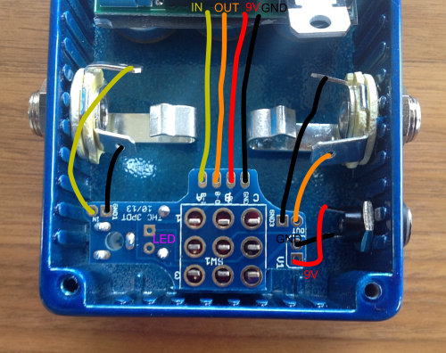
New to KiCAD, been reading through the FAQ and doing a first project (effects pedal). Effects pedals often have a number of PTH. Even this design which is 95% smd has PTH inputs/outputs/led.
Is picking a generic CONN_01 with PTH footprint the best way to do this in EeSchema? I have tried searching for a dedicated PTH schematic, but have come up empty every time.
They are plated through holes that have external lead wires manually soldered to them. They don’t represent a thru hole part (e.g. resistor or electrolytic).
They attach to different jacks. If was to represent them on the schematic as a jack it: 1. doesn’t match the design intent (jack doesn’t go on PCB); 2. I would need to assign multiple PTH footprints to a single schematic, and I don’t know how to do that at the moment.
Open up the footprints and I think you will get a better understanding. You can choose a pad for a single connector. Through hole pads are generally plated by default.
Right. That was what I originally suggested in my first post, using a generic CONN_01 and then a PTH footprint. I was just wondering if there was another way that was best practices?
I presume I can add more than 1 footprint per schematic, yes?
One footprint per symbol. I find browsing footprints easier in pcbnew myself. It takes a while to become acquainted
with what’s available for us newbs.
So for an axial lead resistor there is a 2X PTH footprint in the library for 1:1 between footprint and symbol? I’ve only looked at SMD footprints so far.
Are you trying to specify some holes where you will solder wires that connect to other parts of your system?
If so, it is common to treat it as a connector. The schematic symbol will probably have a designator prefix of “Jx” (e.g., “J3”, “J12”, etc.). Since many input, output, and power connections are actually pairs (e.g., “+12V” and “Return”; “Signal Out” and “GND”; “Right IN”, “Left IN”, and “Common”, etc) a 2- (or 3-) position jack symbol may be appropriate.
I don’t know if KiCAD’s libraries include footprints specifically intended for soldered wire connections. It is easy enough to make such a footprint: It will be a through-hole component, with a generous pad size (to make soldering easy); the pad shape will probably be round or square (Consider using a particular shape to identify the “Ground” connections); the center hole should be sized to accommodate the expected wire gauge (not so small that you can’t get the wire through the hole, nor so large that the wire flops around in the hole with half a pound of solder securing it in place); and you might consider adding some stitching vias around the edge of the pad to increase mechanical strength.
Äh no?! There are proper footprints for THT resistors in the lib. You can however not simply move the holes around freely (ok you can but it is not really suggested to do so.)
See the Resistor_THT lib.
And in general i advice against soldering wires directly to the PCB. If there is any problem with the pcb then you will need to get out your solder iron just to change it. Use a proper connector or at least a screw terminal. Will make your life a lot easier.
Also remember that soldering wires means you weaken them (the solder gets sucked into the wire. The point where the solder ends and where pure copper starts is where it will break if there is ever bending load on the wire. This is why crimping is superior to soldering even for connectors.)
Correct. You can also choose a header pin with more than one connector. Say you have a two wire speaker output. You can choose one footprint with two holes. You don’t have to put the connector on the board but would have that option if you wanted it.
This is 100% the intent. Took me waaay too long to realize I should probably have a connector symbol, and then I was going to find/make large pad PTHs with via stitching, as you suggest. But it seems a good first question to make sure that’s the preferred approach.
You can add 1x1 connectors (one pin in symbol, one pad in footprint) for each wire. But if you put them all side by side it maybe be better to select one symbol/footprint which has as many pins/pads as you need and use 2.54mm pin header footprint. This will be compatible with pin header connectors for which you can find plug/wire cables. So it may give you more to choose from later.
The part you are talking about is very easy to make in the footprint editor but it depends on your comfort level at this point of the learning curve. You can always adjust an existing part too. But chances are there is something already in the existing libraries that fit your need. It will just take some looking to become familiar.
The symbols for BT1 and SW1 are custom creations of my own design. No, this approach isn’t fully compliant with ANSI standards but (in my opinion) it effectively communicates the design intent to the folks most likely to view this document in the future (myself included).
As already mentioned by @Rene_Poschl, I made the connections with pin headers rather than soldered wires. The footprints associated with my custom symbols are just standard footprints for pin headers - though I used right-angle headers due to limited vertical clearance, so the footprint courtyards are extended to accommodate the mating wire housing.
For soldering wires to PCB’s you can start with any connector which has the right number of THT pins for your design.
For example, here I have a 2 pin bent header with a pitch of 2.54mm:
Then hit ‘e’ for edit, and in the “Move and Place” tick on the “Free” radio button.
After that, you can feely move the individual pads of your connector:
Wires soldered directly to a PCB tend to easily break right at the edge where the solder ends and the loose strands begin. Especially if the wires move or there are vibrations.
There are 2 realatively easy fixes for this, and the goal is to not move the wire at exactly that point.
It can be done by putting 2 extra holes in the board, and then threading the ends of the (still isolated) wires through these holes before soldering, or you can glue them to the PCB about 10mm distance from the soldered PTH holes.
Sticking to standards unless you have a really good reason not to gives you options down the line. Also, if you share the project then it gives those folks options too.

 I find browsing footprints easier in pcbnew myself. It takes a while to become acquainted


