I have components on both front and back side of the board. I have chosen components on both sides in the layer setup screen. My version
Application: kicad
Version: 4.0.4+e1-6308~48~ubuntu16.04.1-stable release build
wxWidgets: Version 3.0.2 (debug,wchar_t,compiler with C++ ABI 1009,GCC 5.4.0,wx containers,compatible with 2.8)
Platform: Linux 4.4.0-36-generic x86_64, 64 bit, Little endian, wxGTK
Boost version: 1.58.0
USE_WX_GRAPHICS_CONTEXT=OFF
USE_WX_OVERLAY=OFF
KICAD_SCRIPTING=ON
KICAD_SCRIPTING_MODULES=ON
KICAD_SCRIPTING_WXPYTHON=ON
USE_FP_LIB_TABLE=HARD_CODED_ON
BUILD_GITHUB_PLUGIN=ON
In 3D viewer I have set red colour for paste layers - I don’t see paste layer on the backside, is it a known bug or is it a user mistake?

I cannot test it now. But can it be something wrong in the way you choose the paste layers of the pads?
Mind that you should design your component from the “front view” and while placing it if you Flip it (‘F’) kicad will switch the layers from front->back automatically.
From your second screenshot it is not even remove the solder mask on that pads.
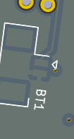
Yes I did place the component on the back layer using F and the PADS are on the back layer when I click them I get PAD on B.Cu.
I didn’t alter anything on the footprint itself, its just a standard Molex pico blade 53261-0271 footprint which came with Kicad. I notice that when I open the footprint in the library I see solder mask/paste etc.
I checked the board layout, the PADS have F MASK, FPASTE un-checked - I don’t remember modifying it.
I just reloaded the footprint from the lib and now I am seeing paste layer on the backside.
I guess its some user error. You can consider this as resolved.
1 Like

