Hi,
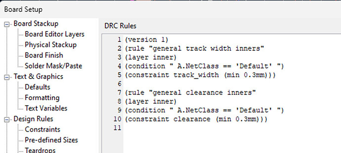
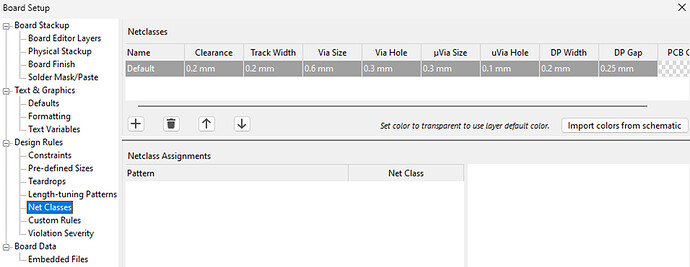
I’m currently working with latest KiCAD version (9.0.5) on a PCB with different copper height on inner and outer layer. Thus, traces on the outer layer (35µ copper) shall be 0.2mm width and 0.2mm clearance (to match device footprints) while on inner layers the limits must be 0.3mm width and 0.3mm clearance (to match production rules).
I already tried the solution proposed here Net classes based on layer - Layout - KiCad.info Forums but I’m stuck with only the clearance being changed, while width is not.
As this shall apply to all nets, I added custom rules to netClass “Default”
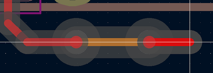
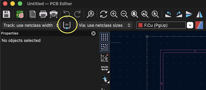
Unfortunately, only the clearance changes while the track width is kept at 0.2mm as defined for default
I’m pretty sure the issue is located between keyboard and chair’s backrest…
Thanks a lot


