Hello,
I would like to create a component (Leds 4 pins) with pins through hole without barrel and top pad on the component side.
How can I just go about it?
I use Kicad V5.1.0.
Thank you.
Hello,
I would like to create a component (Leds 4 pins) with pins through hole without barrel and top pad on the component side.
How can I just go about it?
I use Kicad V5.1.0.
Thank you.
Edit the pins and select the type of pin THT. In the layer list select copper on B.Cu only.
Always helpful if you link to the datasheet of the device that you are talking about. Without this it is sometimes a bit of a guess as to what you are after.
Remember that the copper in the gerbers actually covers the hole and the manufacturer probably interprets it as a normal through-hole with barrel, and they require annular ring in the bottom side. Or they may require some clearance between the copper and the hole. You have to negotiate with them about how to mark them so that they can make it correctly - if they are willing to do it at all.
EDIT: assuming you use a board manufacturer - it’s different if you etch it, of course.
Thank you eelik, you’re right, this is a discussion with the PCB manufacturer, in fact I made a prototype that does not work, when I weld led’s 4 pins, short circuit occur, from one side to the other, this with the “standard” module of Kicad V5. One of the solutions would be to decent the drilling holes, the other, the one I see by only putting welding on one side. Here is my deal.
We need to know what the component is that you want to use
Your explanation is a bit confused. You could make a few screenshots of what you see in kicad and annotate where the shorts are. Or a photo could also show this. I suspect that you did something slightly wrong and your workaround might not be the best option available.
Yes, I agree, but when you order components from China you don’t know exactly what you receive. The fact, I’m using standard module from Kicad V5.0.1 for a RGB Led, at the end, it’s very difficult to sold manually one by one.
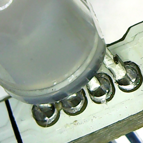
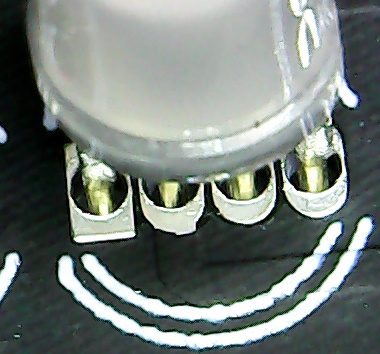
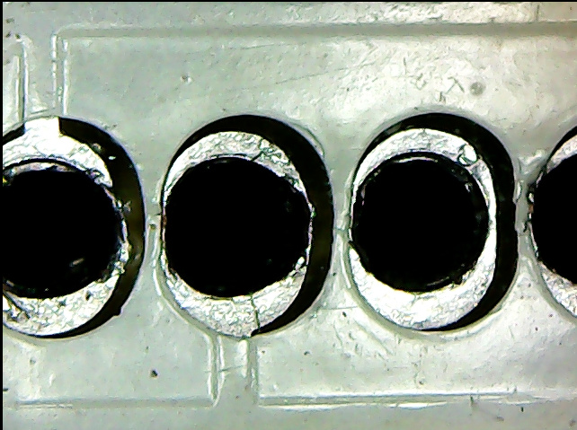
Thank you Rene, nothing is confusing because the pellets are too close and the hole for drilling pines are too big. So I have to check one by one each weld, and despite everything, there are still short circuits that are difficult to find. I made pictures.
A picture would be great, I am trying to guess why a plated hole causes shorts. This must be a very strange part.
I avoid what amounts to single layer board as the solder joints are fragile, even worse I guess with lead free solder
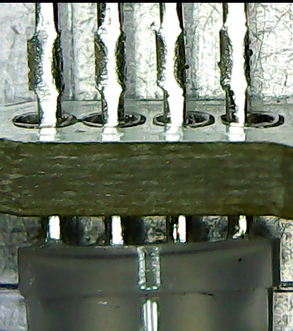
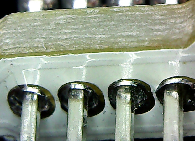
Here are some pictures of the real PCB, you can see a very short distance between the pads!


The footprints you use are for parts with much larger leads. Reduce the drill size and pad size and you should be ok. (Check the datasheet of your device and see what the maximum size of the lead is specified to be. Add a bit to that for solder and the tolerance of your drill sizes and you should arrive at something closer fitting your part. More details on drill size calculation see: Tutorial: How to make a footprint in KiCad 5.1.x (From scratch)?)
Hi Rene, yes that’s I’m doing reducing drill from 1mm to 0.8mm and pads size
Reducing pad sizes will definetly help for your next patch. Using a bit of extra flux combined with a minimum amount of solder will allow you to solder your current patch without trouble. (If you can not solder these huge things forget about soldering any modern integrated circuit.)
And buy good cleaning equipment. Using flux can create a sticky mess that makes it easy for small specs to stick where they should not be. (Like the small metal spec seen in one of your pictures)
Looking at your photos, even 0.8mm is a bit high. LEDs are particularly sensitive to soldering damage, so oversized holes are asking for cooked LEDs
Check your manufacturers requirements for minimum rest solder ring (or annular) as this rule might be violated by your new pads.
A photo might not be the best thing to base this on. For example the knightbrigt LEDs used as the reference for the original footprint have a tolerance range of -0.1/+0.25mm on the leads. ordering a new patch might result in being unable to even get the LEDs in if you decrease the hole size by too much (especially if you also have the combination of getting your holes on the small side of the tolerance range.)
We would need the parts specification documents to make any call on that one.
for reference the knightbrigth pdf https://www.kingbright.com/attachments/file/psearch/000/00/00/L-154A4SUREQBFZGEW(Ver.11A).pdf (drawing is on page 1)
You’re right, ideally it should be better to use the manufacturer’s specifications of Leds. Unfortunately, I do not have them.
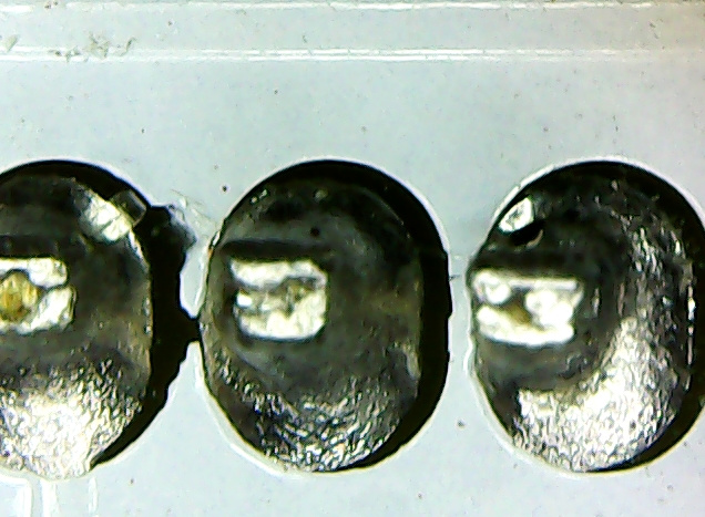
So, in the meantime, I made snapshots of my RGB cube (it’s a Kit that I’ve been working on for a while now), I remove one led and here’s what it looks like: