Hi 1.21G
I’ve seen a few versions of the clamping circuit (seem to deal with AC current ) and am not sure what to choose or how to implement. I’ve tried one…
The DRV8825 is the stepper driver I have been using with a single row header to mount it. If there was a socket this would be great but I don’t think that’s the case.
Adam
Attached is the latest version. Thanks again for all the input!!
Adamsaw_v4.pdf (98.6 KB)
saw.sch (48.3 KB)
Rpi header.lib (302.0 KB)
1 Like
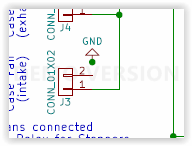
There is a wire missing from J3 pin 2 to GND.
1 Like
There might be a misunderstanding regarding my remark about junctions.
My recommendation was to have a junction in situations like this:

Here (and similar cases) it is unnecessary and even distracting (although it does not do any harm, functionally):

2 Likes
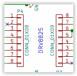
The right side of the DRV8825 connectors P7/P8/P9 is upside down. If the pin numbering of the connectors is meant to be the same as in the DRV8825 schematic.
1 Like
Thanks Martin. Appreciate the eye for detail and info.
Adam
Sorry, my mistake, I was looking at the DRV8825 itself which has 28 pins instead of the breakout board you are using.
You should create a symbol to represent this part with proper pin naming etc. It is a shame they chose to number to two rows of pins with identical numbers but you should number the pins like any other IC. And when the time comes create a proper footprint for this symbol rather than using two single row headers. It will save a lot of confusion on the schematic and be less error prone on the PCB.
As mentioned you’ve gone a little overboard with your junction dots. They are usually only placed at a junction of 3 or more wires, although some people prefer to not have more than 3 wires connecting at any one point.
You can’t have separate grounds the way you are trying to do it. GND and GNDA need to be connected. Although you should route them on the PCB as if they were separate, only connecting them together at the power supply.
I don’t think pin 1 of P4, P5 and P6 should connect to GND. and isn’t pin 7 of these connectors the fault output? Again you should have a proper symbol for the DRV8825.
Your attempt at a clamp circuit is not going to work. But since these are outputs from the Pi you shouldn’t even need the diodes. If you had problems in the past with these outputs it was probably due to poor grounding of the driver modules. If you are concerned about these outputs you could put a 100R series resistor on those pins.
Since you now have CP2 and CP3 you don’t need CP1.
The pull up resistors on your opto outputs should not go to 24V!!
I think your schematic is improving and becoming more readable with each iteration.
2 Likes
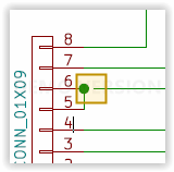
I noticed a gap in the connections ( see below)
Another issue: I take it from the DRV8825 schematic that the DRV8825 module inputs are raw controller inputs directly to the chip. So the diodes D4, … essentially leave the inputs floating when the RPi output is low. They will not pull the module input low. Of course, any voltage building up on the module inputs will be capped by the diodes, but then the RPi logical 0 will not be exactly 0V. Add the diode drop (which is around 0.6-0.7 even at low currents) and this can be a close draw for the 0 logic level at the module input.
The module inputs connected to the capacitors at P7 are left floating anyways.
1 Like
Thanks Straubm.
I have made some changes and with respect to your comment below,
essentially leave the inputs floating when the RPi output is low. They will not pull the module input low. Of course, any voltage building up on the module inputs will be capped by the diodes, but then the RPi logical 0 will not be exactly 0V. Add the diode drop (which is around 0.6-0.7 even at low currents) and this can be a close draw for the 0 logic level at the module input.
Can you kindly recommend an action I should take here? Should I set up a pull down circuit?
All the best
Adam
Here is the latest version. Thanks!saw_v5.pdf (97.7 KB)
There is no action required for this. First of all the diodes are not needed, secondly the DRV8825 has 100K internal pull down resistors.
Looking better. You need to renumber some of the pins on the DRVs, pins with the same number will be assumed to be connected by KiCad.
That’s the solution, to connect directly.
I overlooked an additional issue: the module inputs at the switches SW1-3 need pull downs for the same reason. Anything around 2K2-10K. When routing the board you could implement resistor arrays to save space - if that is an issue.
[EDIT] from 1.21Gigawatts I learned now that the DRV8825 has internal 100K pull downs. So my statement about the inputs to the switches is obsolete.
You still have both “GND” and “GNDA”, I would rename all “GNDA” to “GND”. They can’t be separate but they will need careful routing when you layout the PCB.
I don’t see any reason to have 2 5V regulators. I would remove the 1A regulator and rename all “5VA” to “5V”. You also need a bulk capacitor (10uF - 47uF) and a 100n capacitor on the regulator output. You can also remove the zener that connects to F1.
Clean up your reference ids, the caps with reference id CPn can have a ref id of Cn, but that’s up to you and your preference.
Then have a final check over your schematic.
PS. Give any thoughts to using PWM to control your fans? You could even add a temperature sensor and control the fan speed accordingly. 
Thanks for the information. I will make these changes and will look into PWM.
GPIO18 is the hardware PWM on the Pi.
My fans are 24V and I assume that I will need a separate transistor to handle the fan circuit. I guess there is no way to do this with the ULN2803A chip already there (unless I switch to 5V fans)? Would the chip even handle an output of 0.1A?
Thanks
Adam
The ULN2803 is rated for 50V 500ma so it could probably handle your fans if you used one output per fan.
Thanks. I only see 1 input to the ULN2803 and I have that connected to +5V. Am I missing something? Or were you indicating that I go with 5V case fans?
My mistake. Seems the current flows back to the ULN2803 so it does not matter what the input current is…The +5V is for the logic inside the component.
No, sorry, I am the one who is missing something.  It’s late here and I need to go to bed.
You can’t use the same chip to drive a 24V load as the free wheeling diodes are connected to 5V through the “com” pin.
You could use an output of the ULN2803 to drive a small MOSFET.
There is no logic in the ULN2803, just 8 sets of darlington transistors and free wheeling diode.
Ignore my previous statement about using the ULN2803 to drive the fans. You need to use an intermediate transistor.
1 Like
Thanks Rob.
So then my relay coils will be powered by the 5V from the ULN2803 and should be connected to ground instead of +5V.
My mistake again. Just found an erroneous +5V connection at the relay coil.


