Hello everyone!
I am using Kicad version 4.0.7
I have been working on a design in Eeschema for quite a while now and I also have started to lay out the PCB in Pcbnew.
This is not my first design I have been working on, but it is the first time that a strange, annoying bug occures (apparently):
The circuit I made in Eeschema includes positive and negative supply voltages ("+VDC" and “-VDC”) and ground (“GND”), plus several other connections, each labeled individually.
When I generate the netlist (as Pcbnew default format) and import it into Pcbnew,
the “-VDC” supply voltage net is not showing up in Pcbnew (and is apparently not included in the netlist, as far as I can tell with the help of a text editor).
All pins which are supposed to be connected to the “-VDC” net are instead connected to the “+VDC” net!
I changed the power supply voltage items several times in Eeschema and I always used default items from the Kicad library, from “VDD”, “VEE” over “+VDC”, “-VDC” to individual net labels,
but there just won´t appear any of the negative power supply nets in Pcbnew.
All positive and negative power supply voltage nets stay connected to “+VDC”.
I tried every option in the netlist import dialogue.
To me it seems like a strange bug, or just an error on my side, but for now I have no Idea what is left to try…
I doubt many will be able to help with your problem as 4.0.7 is very old.
It would pay you to upgrade your version to 5.1.10 then see if the problem persists.
You can find 5.1.10 here: https://www.kicad.org/download/
Power supply nets are global labels in kicad. Any net can only ever have one name. If you therefore connect any two global labels with differentt names (like vcc and +vdc) then the resulting net will have only one of these names. Which one gets choose is not well documented.
Something to keep in mind is that any invisible power input pin is a global label. So if you have a symbol with an invisible power input pin with name vcc (like sadly some of the symbols for logic ICs) and then connect this to your +vdc net then you end up with such a conflict.
For me it looks like you have copied +VDC symbol and changed its name to -VDC. But the symbol name is not what KiCad looks to set the net to connect the wire ended with that symbol to. Look deeper inside that symbol.
Switching to V5 (V6 soon) is really a good move.
When I started to use KiCad it was 4.0.6 -> 4.0.7 moment. I remember that for example via-stitching was not solved correctly in V4 and you have to use way-arounds. It was something what made me to go to V5 when it was close to first release.
Thanks, Rene_Poschl!
I will stay with my current version until the project ist finished, unless I get really stuck.
To be more clear (just for anyone, who has a similar problem and gets to read this, not against you): I have only ONE positive and ONE negative supply voltage in my design at a time.
I changed them always simultanoiusly.
So there does not exist a “VDD” net at the same time as a “+VDC” net, the same with the negative voltages.
The point with the hidden power pins on the IC symbols is a good point, but I revealed all hidden pins in the design (I checked the option), and I am only using analog linear ICs and transistors.
Thanks, Piotr!
Also, just to be clear:
I have not copied and renamed the power supply symbols (except one time when I created dedicated global labels for the supply voltages instead).
But the VDD / VEE and +VDC / -VDC symbols were taken directly from the library and interchanged respectively.
I will try again for a little while and maybe I will move to a newer version of Kicad.
Two different nets that get connected together is indeed usually user error, and a quite common error too, so it likely has nothing to do with your old KiCad V4.0.7.
One common way to make this error is to draw a wire right through a decoupling capacitor between the +VDC and -VDC nets. Most of such a wire overlaps with the capacitor symbol itself and is therefore hard to spot on the schematic.
Also any place where your +VDC and -VDC nets come close together it’s easy to make a similar mistake.
So use the highlight net function and then zoom in and carefully inspect where your wires go on the schematic. Pay special attention to any junction dot you see. Junction dots right on the attachment points of pins are especially suspicious.
In the meantime I have made several electrical rules checks and I did not get an error with the positive and negative power nets.
I also have made a new test project with a simple schematic, which worked out fine in Pcbnew.
After that I imported one sheet of the real schematic into a new blank project, made the annotation and exported the netlist.
When I imported this netlist into a new blank PCB, it showed the same missing negative power net as in my real project.
So I guess the reason is buried somewhere in the schematic or project file.
During the ERC in the real project, I also got some strange warnings that told me, some parts were not connected (for example capacitors and GND symbols, or +VDC symbols and IC power inputs), although these parts have successfully been connected in my PCB before…
I hope it is just a mistake on my side
and that someone else out there will learn from this, too.
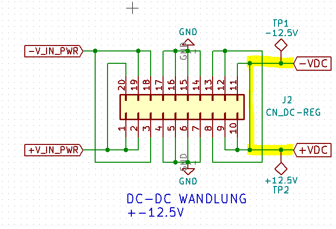
Well… it was indeed my fault!
There was an unnnoticed and unintended connection between the positive and negative supply rails,
right at the DC-DC converter, see the picture!
This must have happened during one of the endless night shifts…
I am so happy that I found it.
This was a good lession for me to go over it again and again, until the fault has been detected.
But now I also know that Kicad won´t let me connect these crucial power supply nets and turn my PCB into a firework.
Thank you all for your quick support!
I wish you all the best and success with your projects!!!
