Device library proposal

Hi,

Recently, I thought a bit about how to optimize part library handling for pcb design tools:

For handling a device one may need the following

  • schematic symbols in different (package) variations
  • footprint(s)
  • 3D CAD files of the package(s)
  • simulation model(s) (electronic, mechanical, thermal)

Currently, KiCad handles this in different libraries and files, which makes things a bit difficult, especially for more complex devices such as a microcontrollers that are available in different packages. My experience is that you often need to create everything for a device on your own and even if there is a footprint with the correct name, it may not fit to the variation the device uses (pad dimensions, thermal vias, …) as packages are often device or manufacturer specific.

Idea:
Pack everything for a device into a single file and no longer separate footprints and symbols in different databases. A user then may download a single file for the part he is interested in (perhaps even created by the chip manufacturer) and has evertything he needs for the part. When selecting a part in the schematic design phase the package is also selected immediately. The package assign step after the schematic is ready would be eliminated. And for each device you would have the perfect footprint. Once KiCad supports circuit simulation, a device file may already include the simulation model.

The disadvantage is of course, that reusing packages is becoming more difficult, and as each device has to deliver its own footprint/package data, the total library file size will increase.

So, what do you think?

Regards,
Josef

Well… who’s going to make those files for ALL possible resistor values?

One for 4.7k, one for 100R, one for 1M, one for 91R…

The problem you have “need to make symbols/footprints myself, even if publicly available” won’t be solved by “lumping symbols/footprints/3d models together in one big database”…

So far I did make all the symbols and footprints I use myself… and 3d models I only reused the resistors.
I don’t trust the stuff that’s available.
And the only thing that would make my life a bit easier would be a better footprint editor and some more consistency in workflow for eeschama/symbol editor and pcbnew/footprint editor.

They’re already working on getting rid of cvpcb and having a more direct link between symbols/footprints as this makes more sense for most people. You then chose the package within the symbol editor and it is linked there, not later with cvpcb.

Conclusio: I like to keep the basic pieces separate - if there must be stronger links the way of approach taken now is OK (linking of footprints in symbol editor).


PS: if anyone sees some 3d model he likes in the pic, just contact me, I’m happy to share.

What I think we need is a good parts manager which can be used to pick a symbol, footprint, 3d model, suppliers, whatever, create a database entry with your internal part number, and copy all relevant files to the project directory and with the appropriate associations inside the files (for example 3d models for footprints). That would also make BoM generation and ordering easier but it’s a pretty big job and not trivial to get working well.

[quote=“Andy_P, post:4, topic:1574, full:true”]
I suppose I should say that library management is the bane of every CAD user and every CAD tool developer. There is no way to satisfy everyone . . . . [/quote]
That is definitely true! It starts with the diversity of users - a hobbyist wants to knock out a board in an afternoon and get parts ordered from a favorite supplier ASAP; a large corporation wants a seamless interface to an integrated system for configuration management, purchasing, inventory control and manufacturing (as well as backwards compatibility with systems that previously performed these functions); and a manufacturer wants footprint information fine-tuned to his particular process and equipment. We could start to list other reasons why this is so, but in the end we must concede that there isn’t a single solution meeting even the most basic requirements of the majority of users.

In a practical sense, there really isn’t a list of “standard” footprints. I routinely use different footprints for the same component, based on whether the board will be soldered by hand, or on automated machinery. Sometimes it makes a difference depending on which automated line will be used to assemble a board - some pick-and-place machinery requires a larger “courtyard” around a component than others. Or, with thru-hole parts you may have two or more footprints with slightly different hole sizes, based on the “standard drill racks” at different board fabrication houses. And there are situations like the standard TO-92 package - with 0.050" (1.27mm) lead spacing it is problematical to maintain both adequate annular and pad-to-pad spacing, so some folks spread the leads into a triangular pattern of some convenient (but not standardized) dimension while others form the leads into a wider spacing but retain the in-line configuration.

As a circuit designer I often want to keep part designations as generic as possible in the early design and prototyping stages. At that stage my superannuated mind can only grasp that I want something like, say, a TL074 opamp, and I’m quite happy to postpone the agony of determining which package style (of 3 or 4 options) to use until a later stage of the development process.

I have long ago conceded that somewhere between 15% and 75% of the time spent to lay out a PWB will be spent in “library work”. It’s not that I distrust others’ libraries - though some are constructed to more rigorous DRC standards than others, and I occasionally DO find outright errors. It’s the fact that 3rd-party libraries weren’t created under the same local constraints that I work with on a particular client or project.

For these reasons I think the current KiCAD workflow has merit. You CAN link a schematic symbol with a particular package in the symbol’s definition file, or you can leave the association undefined until a later time. I just wish there was a more efficient way of cataloging and searching for the particular item you’re seeking.

Dale

Heh - if you script it it’s trivial. My VRML model scripts create something like 4000+ THT resistor models faster than you can blink - but if you tell an EE that you have 4000+ resistor symbols to choose from you can bet someone will be laughing.

I have worked with a few systems that tried to do some (or all) of these tasks, and I don’t think ANY of them worked “well”.

Dale

100% this, but who said the development and evolution of KiCAD was at the finish line yet… so lot’s of room for improvement… maybe not next week, but some when next year or thereafter.
Already amazing what one can do with this software.

You are right. But you could handle these generic parts the same way it is done today: You may still be able to define some parameters such as ‘value’ for the part. You would simply have to make one generic device for R, C, L, …

And if you need some more specific part such as a high precision resistor from a specific manufacturer, you might add a second device file to your library containing for these parts with some additional information (such as package 3D-Models, simulation model) from a specific manufacturer, but still with configurable value parameter.

That’s true, but it would simplify handling them, if you have one ‘collection’ for each part.

Yes, optimizing the symbol and footprint editor and their workflow would help a lot.

True, but how many variations of SOIC-14 do exist out there? In practice, you nearly always have to create a footprint specifically for a device.

And, the OpAmp is a good example why completely generic symbols are often impractical: Because most OpAmps come in packages with multiple of them, and you will have to assign the pins of them in schematics phase. And this often also fixes the package options that are left, because different packages may have different pin assignments or even pin counts. Today, this means to create multiple symbols for different package variations.

That’s a good point. I have no experience in automated PCB manufacturing, but wouldn’t it be possible to use parameters for these information?

Well, open source might be a solution to this - if it is done right. If you would have an open standard for part libraries that really work, it might even adopted by the industry.

Hi,
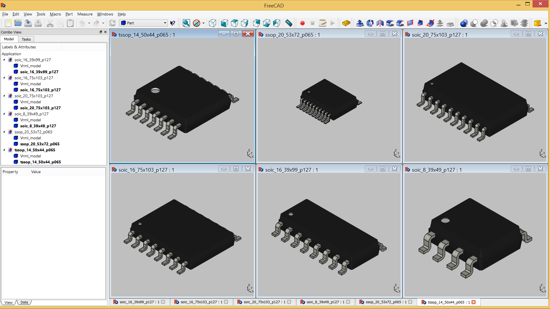
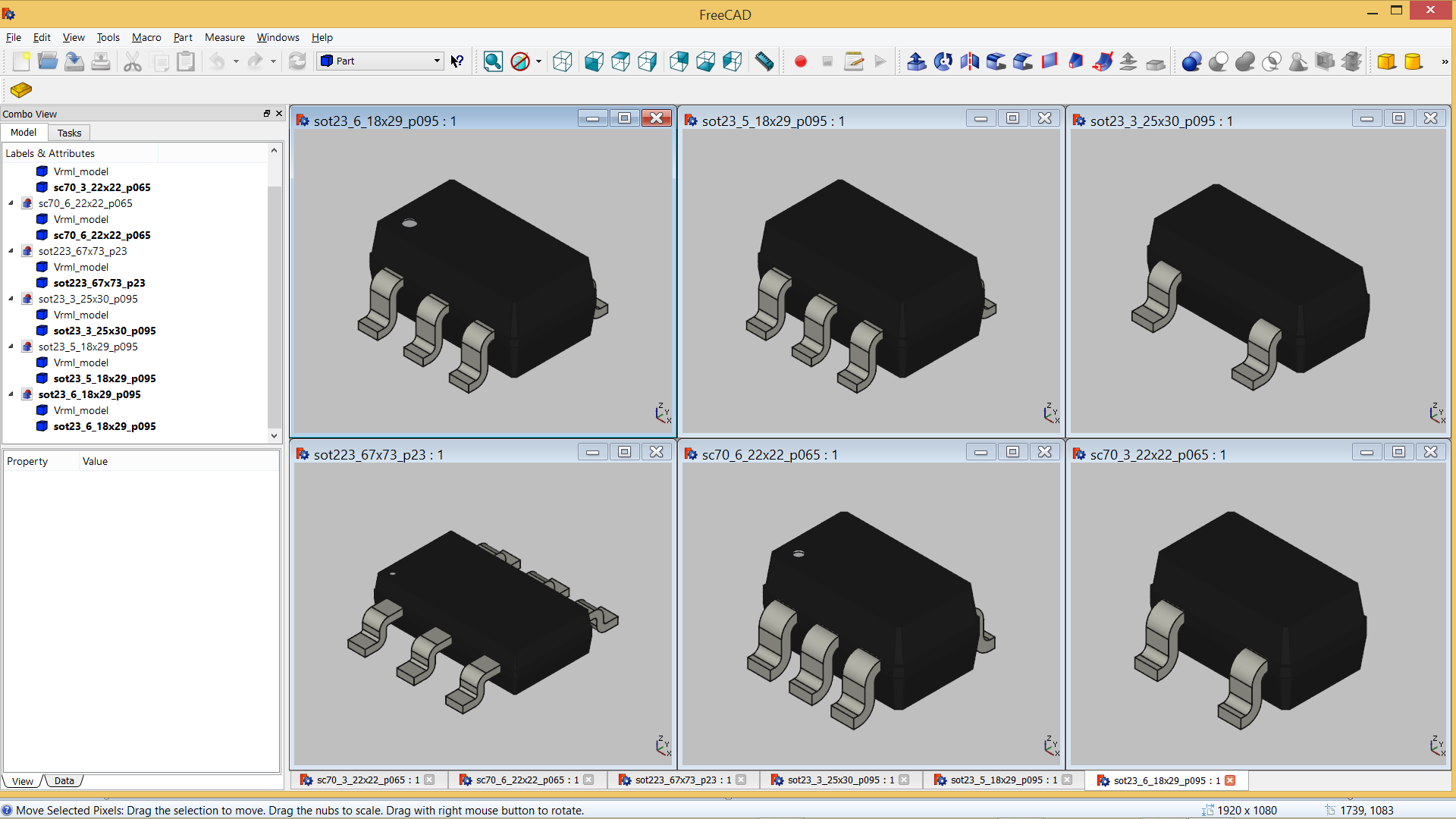
if you need some parametric 3D models (dimensions as per data sheet of manufacturer) here you can find some:
https://github.com/easyw/kicad-3d-models-in-freecad/


Maurice

1 Like

I certainly didn’t mean to even imply that KiCAD was a polished final product, ready for display and critical examination by any and all evaluators.

As the old camel trader said, “Only Allah is perfect!”. With CvPCB gone as a stand-alone program and its function absorbed into EESchema I don’t see a strong justification for putting resources and effort into revising the process of assigning footprints. There are bigger bugs to squash, and a few corners that still need to be rounded over on this wheel. After the rest of the program has solidified, and a well thought-out concept for library organization and administration emerges, the footprint-assignment problem can be reconsidered.

Dale

Sorry, didn’t meant to imply that… was merely me ‘thinking’ loud… :wink:

Thanks, that looks like a really nice collection of scripts. I would like to see this kind of data embedded in a device-file (or maybe call it device-package/archive). And then interfacing tools like FreeCAD directly from KiCad. Similar things could be done for SPICE simulation. KiCad does not need to integrate every feature, it could just be the place to collect all information for a project.

I’m glad I’m not the only one who insists on making his own symbols and footprints. After all it’s really not big deal with KiCad. Locking footprint with symbols though is a proposal I would not support. In general I can assign 60% - 80% of all footprints (CvPcb) to a given schematic within 5 minutes from existing stock. There is nothing wrong with this concept. As the number of symbols and footprints grow and you want to add datasheets(links), 3-D models distributors etc. a db-based solution (thanks cbernardo) is advisable. To make this powerful and usable is not a small task.

1 Like

Just went over a parts list of a smaller project (ca. 140 parts). Of the 47 caps 29 in the 0805 housing, of the 40+ resistors about 40 in the 0805 housing. All semis standard housing and interchangeable with other models. And yes, at almost any stage of the project I take the liberty to change an op-amp, for cost or performance reasons. Not only in a few cases values of components are being changed any time, more likely towards the end of a development cycle. That’s not ridiculous to me. Take a 555, comes from many different vendors with different names. The basic principles of software design would be violated by hardwiring symbols, values and footprints. That’s taking away a degree of freedom which many of us don’t want to give up. After all the intend is to minimize the number of symbols and footprints to the bare minimum.

From an app designer’s point of view, there are many issues here: the data model, the user interface, the implementation, the architecture…

The OP might be suggesting a user interface: “For my design (document) I want to be able to choose one thing (say from a list) that adds all the design data (the schematic symbol, package footprint, 3D model, and simulation data) in its default (generic, typical, up-to-date) form. Later, I want to refine the choice by choosing different other design data that is still compatible. But I also want to choose what the default is (for my shop) and only see choices whose packages are still available in my shop’s stock or from stock of my shop’s set of distributors.”

As other’s have said, it’s probably doable but it probably involves new data model relationships (for example a dated association between a distributor, a package, a shop.) It might be a separate app from KiCad. It might require changes to KiCad. It might require changes in how the industry publishes data.

It is horribly complex. It’s not just: let’s change KiCad.

An op-amp is not the best example, but a 2p switch or pushbutton? You have a single schematic symbol and may use thousands of possible parts. Most of times they will require a new footprint created by your own hands.
A schematic component definition should contain a list of zero, one or more footprints. E.g a 2 pin-switch component should be empty (always “casual”), a MCU should have one footprint pre-set (I mean no need to set footprint after placing this schematic symbol), and “R” should have 10-20 different packages on the list to pick (“1206”, “0805”…). If I place a resistor and choose “0603” as its footprint, let it be saved as default, then my next “R” will get the same fottprint by default…

(In real I place a “R”, fill the value, footprint etc, then create more resistors by C copying, so it is only a wishlist item, and not really important now.)

So, KiCAD gives you the liberty to do it exactly like that afaik and it also gives @novaktamas or @maxwaldo the liberty to have the ability to change…
I mean, one doesn’t preclude the other really.
There is more important stuff wrong with library management usability wise than arguing about which way to Rome is the best.

You are right Joan, I regarded assigning 0/1/n footprint to schematic components as a very low-priority wishlist item.
I myself prefer a single pushbutton schema component, then filling footprint later, but we have the freedom to create different components for “10kohm 0805” and “4k7 0805” and so on.
It really depends on the frequency of using the same component. I practically never re-use the same tactile button, so I prefer an empty footprint for SPDT.

This object is very over-discussed, so Ufff this was my last word on this :speak_no_evil: